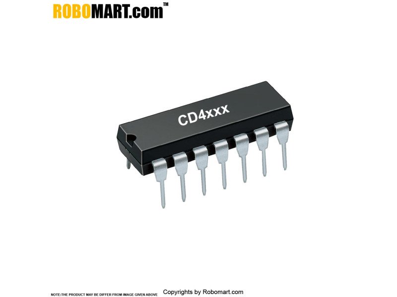
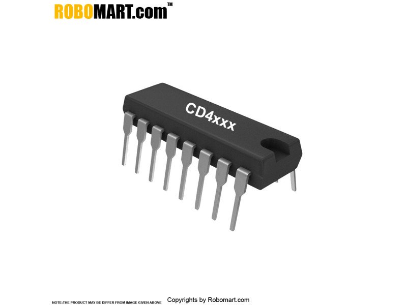
CD4066 Quad Bilateral Switch

CD4066 Quad Bilateral Switch
₹ 29.00
- Stock: In Stock
- Brand: Generic
- SKU: RM001656
Warehouse Code: R00009-S06-P05-Z01
Package/Case: PDIP (N) | 14
IC Name: CD4066
The CD4066B is a quad bilateral switch intended for the transmission or multiplexing of analog or digital signals. It is pin-for-pin compatible with the CD4016B, but exhibits a much lower on-state resistance.
Features of CD4066 Quad Bilateral Switch:
- 15-V Digital or ±7.5-V Peak-to-Peak Switching.
- 125- Typical On-State Resistance for 15-V Operation.
- Switch On-State Resistance Matched to Within 5 Over 15-V Signal-Input Range.
- On-State Resistance Flat Over Full Peak-to-Peak Signal Range.
- High On/Off Output-Voltage Ratio: 80 dB Typical at fis = 10 kHz, RL = 1 k.
- High Degree of Linearity: < 0.5% Distortion Typical at fis = 1 kHz, Vis = 5 V p-p, VDD–VSS .
- Extremely Low Off-State Switch Leakage, Resulting in Very Low Offset Current and High Effective Off-State Resistance: 10 pA Typical at VDD–VSS = 10 V, TA = 25°C.
- Extremely High Control Input Impedance (Control Circuit Isolated From Signal Circuit): 1012 Typical.
- Low Crosstalk Between Switches: –50 dB Typical at fis = 8 MHz, RL = 1 k.
- Matched Control-Input to Signal-Output Capacitance: Reduces Output Signal Transients.
- Frequency Response, Switch on = 40 MHz (Typical).
- 100% Tested for Quiescent Current at 20 V.
- 5-V, 10-V, and 15-V Parametric Ratings.
Applications of CD4066 Quad Bilateral Switch:
- Analog Signal Switching/Multiplexing.
- Signal Gating, Modulator, Squelch Control, Demodulator, Chopper, Commutating Switch.
- Digital Signal Switching/Multiplexing.
- Transmission-Gate Logic Implementation.
- Analog-to-Digital and Digital-to-Analog Conversion.
- Digital Control of Frequency, Impedance, Phase, and Analog-Signal Gain.
Also Searched as : CD4066 IC.
*Note: Product may be differ as per shown in image
SKU: RM001611
The CD4016BC is a quad bilateral switch intended for the transmission or multiplexing of analog or digital signals. It is pin-for-pin compatible with ..
₹ 29.00
( + 18% Gst Extra )₹ 34.22 (Inc GST)
SKU: RM001643
The CD4052 is a 4 channel analog multiplexers and de-multiplexers are digitally-controlled analog switches having low ON impedance and very low OFF le..
₹ 29.00
( + 18% Gst Extra )₹ 34.22 (Inc GST)
SKU: RM001644
The CD4053B is a 2 channel analog multiplexers and de-multiplexers are digitally-controlled analog switches having low ON impedance and very low OFF l..
₹ 29.00
( + 18% Gst Extra )₹ 34.22 (Inc GST)
SKU: RM001657
The CD4067B CMOS analog multiplexers/demultiplexers are digitally controlled analog switches having low ON impedance, low OFF leakage current, and int..
₹ 49.00
( + 18% Gst Extra )₹ 57.82 (Inc GST)


